By Ripon Kumar Dey, PhD — Nanofabrication & Photonics Scientist
Most explanations of augmented reality displays start with the optics — étendue, waveguides, diffraction gratings — and treat the physical structures that create those effects as a black box. That’s a reasonable place to start if your job is deciding which architecture to bet on. But I’ve spent the last decade on the other side of that black box: in the cleanroom, patterning the nanoscale gratings that actually make a waveguide work. This post walks through the same core optical concepts that govern AR displays, but with an eye toward the question I find most interesting — not just what these components need to do optically, but what it actually takes to build the nanoscale structures that do it, and where that fabrication reality quietly shapes the optical design choices made far upstream. I’ve written this to be readable without an optics background, though I won’t shy away from the underlying physics where it actually matters to the engineering decisions.
This is a long piece, split into two halves. The first half covers the optical fundamentals — pupils, étendue, total internal reflection, diffraction, coherence, polarization, and how photons get generated in the first place. The second half is where I think the more interesting material lives: how those optical requirements translate into an actual nanofabrication process, what can go wrong at the wafer scale, and how a defect a few hundred nanometers wide can determine whether an entire product ships on schedule.
Part One: The Optics
1. The problem AR glasses are trying to solve
A pair of AR glasses needs to inject a digital image into your eye while leaving the real world visible behind it. The most direct way to do this — a small projector held in front of your eye, the way a slide projector throws an image onto a screen — works fine on an optics bench, but the geometry doesn’t survive contact with a real face. To understand why, it helps to be precise about what your eye is actually doing when it looks at something.
When you look at a real object, every point on its surface scatters light outward in a diverging cone. The closer the object, the more sharply that cone diverges. Your eye’s lens takes those diverging rays and bends them back down to a point on your retina, and your brain interprets that convergence as “an object exists there, at that distance.” A display has to fake this same divergence to convince your eye it’s looking at something real rather than a flat picture. An image formed this way — one your eye reconstructs from rays that only appear to originate from a point in space, without any screen or surface actually existing there — is called a virtual image, in contrast to a real image, which is one you could genuinely capture on a physical screen because the rays actually converge there. Every AR and VR headset on the market forms a virtual image; that’s true regardless of which architecture it uses to get the light to your eye.
Pupils, apertures, and the eyebox
Every optical system has a limiting aperture — the physical opening that bottlenecks how much light gets through, whether that’s the iris of a camera lens, the frame of a telescope, or the edge of a waveguide. Optical designers talk about “pupils” rather than apertures because what matters isn’t the physical opening itself but its image, as seen from either side of the system. The entrance pupil is what that limiting aperture looks like from the object side; the exit pupil is what it looks like from the image side — the side where your eye sits. In a near-eye display, the exit pupil is the specific patch of space where your own eye’s pupil needs to be for you to see the full image without vignetting (part of the image getting clipped at the edges).
Because your eye is never perfectly still — it rotates, the glasses shift slightly on your nose, your pupil itself moves a couple of millimeters as you look around — a single point-sized exit pupil is nearly useless in practice. What you actually need is a three-dimensional volume within which your eye can wander while still seeing the complete image; this volume is the eyebox. A generous eyebox is forgiving of normal head and eye movement. A stingy one demands the headset sit in exactly the right position, and any drift causes part or all of the image to disappear. This turned out to be the practical failure mode of some of the earliest slim smart-glasses attempts, which used very compact, fixed-pupil optics: the image looked sharp when you stared straight ahead, but a small eye rotation was enough to lose it entirely.
2. Étendue: the conservation law that won’t let you cheat
The reason you can’t simply shrink a projector and keep both a wide field of view and a large eyebox comes down to a single conserved quantity called étendue (from the French for “extent”). Étendue is the product of the area a light beam occupies and the solid angle over which it spreads — loosely, how much space the light takes up, multiplied by how spread-out in direction it is. Any lossless optical system — a stack of lenses and mirrors with no light absorbed or scattered away — conserves étendue exactly. You can redistribute it between area and angle, but you cannot shrink the product.
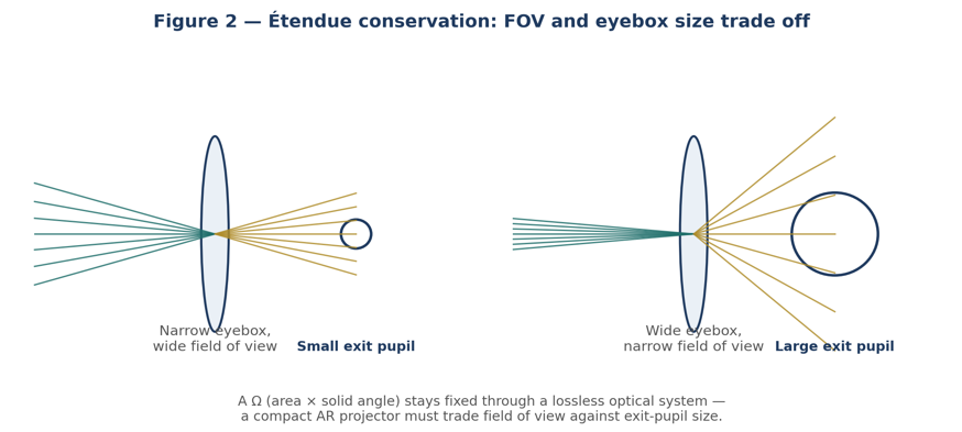
Figure 2. Étendue conservation: a compact optical system can deliver a wide field of view or a large exit pupil, but not both at once.
This has a very concrete consequence for AR optics. Field of view is fundamentally an angular quantity — how many degrees of your vision the display fills. Exit pupil size is an area quantity — the eyebox we just discussed. Because their product is fixed by the étendue of your source, pushing one up necessarily pushes the other down, for a given projector size. A compact, temple-mounted projector has small optics, which caps its étendue budget; the designer is then stuck choosing between a wide field of view crammed through a small, unforgiving exit pupil, or a comfortable eyebox purchased at the cost of a narrow, tunnel-vision field of view. You cannot buy your way out of this with cleverer optics alone — only by growing the physical system, which is exactly what the glasses form factor won’t allow, or by getting cleverer about how you deliver and multiply the light. That second option is where waveguides come in.
3. Total internal reflection: trapping light without losing it
Before getting to waveguides directly, it’s worth being precise about the physical mechanism that makes them possible: total internal reflection, or TIR. When light traveling inside a denser medium (like glass, with refractive index n1) hits a boundary with a less dense medium (like air, n2), part of the light typically refracts through the boundary and part reflects back — the everyday behavior you see looking into a window at night, both transmitted and reflected. As the angle of incidence increases, the refracted ray bends further and further away from the boundary’s normal, until at some critical angle, θc = arcsin(n2/n1), the refracted ray would have to bend a full 90° — meaning it travels exactly along the surface. Beyond that angle, refraction becomes physically impossible, and all of the light reflects internally. No absorption, no partial transmission — it’s a lossless, perfect mirror created entirely by geometry and the difference in refractive index.
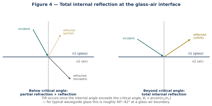
Figure 4. Below the critical angle, light partially escapes through refraction. Beyond it, the boundary becomes a perfect mirror — total internal reflection.
For a typical waveguide glass with a refractive index around 1.5–1.9 against air, the critical angle works out to somewhere in the range of 30°–42°, depending on the specific glass formulation. This is the same physical mechanism that keeps light confined inside a fiber-optic cable over kilometers with minimal loss, and it’s what allows a thin sheet of glass to act as a lossless conduit for image-bearing light, provided the light is coupled in at a steep enough angle to begin with.
4. Diffraction: bending light with structure instead of curvature
A conventional lens redirects light through refraction — a gradual bending as light crosses a curved boundary between two materials of different refractive index. Diffraction is a different mechanism entirely, and it only shows up when light interacts with features on the scale of its own wavelength — for visible light, a few hundred nanometers. At that scale, light can no longer be treated as a simple ray traveling in a straight line; you have to account for its wave nature, and specifically for how many overlapping wavelets interfere constructively and destructively as they pass a periodic structure.
A diffraction grating is exactly this: a periodic structure, spaced on the order of the wavelength, engineered so that light bends predictably at specific, discrete angles rather than the continuous range you’d get from ordinary refraction. These discrete output directions are called diffraction orders, conventionally numbered …, −2, −1, 0, +1, +2, … where the zero order simply passes straight through undeviated, and each other integer order bends by an angle set by the grating equation:
Λ (sin θm − sin θi) = m λ
where Λ is the grating period, θi and θm are the incident and diffracted angles, m is the order number, and λ is the wavelength. The practical takeaway is that the grating period controls how sharply light bends, and — critically — that angle depends on wavelength, meaning red, green, and blue light diffract to different angles from the same grating. Managing this wavelength-dependent spread (called dispersion) without introducing visible color fringing is one of the harder systems-engineering problems in waveguide combiner design.
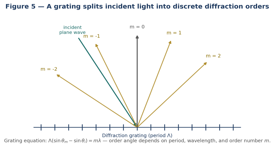
Figure 5. A periodic grating splits an incident beam into discrete diffraction orders, each bending by an angle set by the grating equation.
Gratings also come in two broad diffraction regimes, distinguished by how strongly they interact with light. Raman-Nath gratings, typically produced when the refractive-index contrast between the grating material and its surroundings is large (glass against air, for instance), spread energy across many diffraction orders simultaneously and work over comparatively wide ranges of angle and wavelength — useful when you need broad coverage, harder to keep tightly efficient. Bragg gratings, by contrast, are engineered so nearly all the energy goes into a single order, but only within a narrow angular and spectral window centered on what’s called the Bragg condition; step outside that window and the grating simply stops diffracting efficiently. This distinction — one grating type trading breadth for flexibility, the other trading breadth for efficiency — turns out to map almost directly onto the two dominant ways of physically manufacturing a grating, which is where the story shifts from optics to fabrication.
5. Waveguides: relocating the projector, not shrinking the physics
The industry’s answer to the étendue trap doesn’t cheat the physics — it works around the geometric constraint instead. Rather than parking a bulky projector directly in front of your eye, you tuck it into the temple of the glasses and use a thin sheet of glass — the waveguide — to carry the image around to where your eye actually is, using exactly the TIR mechanism described above. Light from the projector enters the waveguide through an in-coupling grating patterned at one edge, which redirects it to an angle steep enough to totally internally reflect. It then propagates down the length of the glass, bouncing losslessly between the two surfaces, until it reaches a second, out-coupling grating, which extracts it back out toward the eye.
The genuinely clever part is what the out-coupling grating does beyond simply redirecting the light once. Rather than acting like a single mirror, it interacts with the propagating beam repeatedly as the beam passes underneath it — extracting a little energy at each interaction point rather than all at once. The net effect is that a single narrow beam gets sampled and re-emitted many times over as it crosses the grating region, producing many spatially separated copies of what would otherwise be one small exit pupil. Stack those copies side by side and you get a large, forgiving eyebox assembled from many small ones, all without growing the physical size of the optics — a direct, physical workaround to the étendue limit discussed earlier, achieved by trading a single high-quality pupil for many lower-intensity replicated ones.
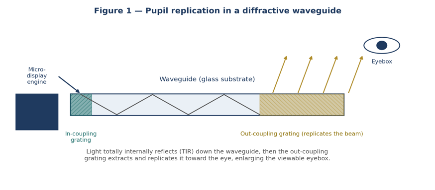
Figure 1. An in-coupling grating redirects the projector’s light into total internal reflection; an out-coupling grating extracts and replicates it toward the eye.
This replication comes at a real cost, worth stating plainly: splitting one beam into many means each copy carries less energy than the original, so the optical engine driving the display has to produce substantially more raw brightness than you’d naively expect from the on-eye image alone. Every additional stop of eyebox you buy through replication is paid for in source brightness and power draw — which is part of why display-source efficiency, covered later in this piece, is such a persistent bottleneck in the field.
6. Coherence: why some light sources cause artifacts and others don’t
Coherence describes how well-ordered a light field is — specifically, its capacity to interfere with itself constructively or destructively. It comes in two flavors that matter for different reasons in a display system. Temporal coherence measures order over time, quantified by the coherence length: the maximum path-length difference over which light can still interfere with a delayed copy of itself. A laser, which emits light at an extremely narrow range of wavelengths, has a long coherence length and can interfere with itself even after traveling very different path lengths — which is exactly what produces the grainy, sparkling artifact called speckle when coherent light scatters off a rough surface or interacts with a diffuser. An LED, by contrast, emits over a much broader spread of wavelengths, giving it a short coherence length that washes out most interference effects before they become visible.
Spatial coherence measures order across the width of the beam rather than along its path. A vanishingly small, point-like source has high spatial coherence, because every part of the beam originates from essentially the same location and stays mutually correlated. As a source grows physically larger, different points on it emit light that’s no longer well correlated with each other, and the resulting mutual interference degrades contrast and resolution — this is one reason microdisplay pixel design and source size matter so much for perceived image sharpness, independent of the raw pixel count.
In a waveguide combiner specifically, both forms of coherence interact with the grating physics discussed above in ways that aren’t always intuitive: a highly coherent laser source paired with a Raman-Nath surface relief grating, for instance, is a common recipe for visible speckle, while the same grating driven by an incoherent LED source may show none at all. Matching source coherence properties to grating type is a real, first-order system design decision, not an afterthought.
7. Polarization: the property everyone assumes but rarely checks
Light is a transverse electromagnetic wave, meaning its electric field oscillates perpendicular to its direction of travel. Polarization describes the geometric pattern that oscillation traces out — linear, if the field stays confined to a single plane; circular, if it rotates uniformly as the wave advances; or the general case, elliptical, which covers everything in between. Unpolarized light is really just a rapid, random mix of all these states averaging out to no net structure.
Nearly every component in a waveguide combiner — the microdisplay itself, the diffraction gratings, any polarization-sensitive coatings used to manage stray light — has efficiency and behavior that depends on the polarization state of the light hitting it. A grating optimized for one polarization can perform dramatically worse for the orthogonal state, and mismatches compound as light passes through multiple components in sequence. Getting this right in simulation is one challenge; getting it right on a physical part, where fabrication tolerances, birefringence in the substrate material, and mechanical stress can all subtly shift polarization behavior from the ideal design, is a substantially harder one — and it’s a recurring theme in why parts that perform beautifully in simulation sometimes underperform once actually built.
8. Where the photons actually come from
Stepping back from the optics entirely: before any of the mechanisms above can do anything, something has to generate the photons in the first place. Both LEDs and semiconductor lasers — the two dominant AR display source technologies — rely on the same underlying structure, a p-n junction: a boundary between an n-type semiconductor region, which has an abundance of mobile electrons, and a p-type region, which has an abundance of vacant lower-energy states (“holes”) for those electrons to fall into. Driving a current across this junction forces electrons into an excited, high-energy state; as physical systems tend toward stability, those electrons eventually drop back down, shedding the energy difference as a photon whose wavelength is set by the material’s bandgap.
When that drop happens spontaneously and independently for each electron, the process is called spontaneous emission, and it’s what LEDs are engineered to maximize — the resulting light radiates over a broad angular range, is unpolarized, and has short coherence, all fairly favorable properties for reducing artifacts, at the cost of being harder to collect and collimate efficiently. A laser instead relies on stimulated emission: an incoming photon of the right wavelength triggers an already-excited electron to drop and emit a second photon that’s a near-perfect clone of the first, matching its wavelength, phase, polarization, and direction. Enclose a p-n junction in a resonant optical cavity that bounces photons back and forth through the active region repeatedly, and each pass triggers a further cascade of stimulated, synchronized emission — the physical origin of a laser’s narrow angular spread, precise wavelength, and long coherence length, the same coherence that reappears later as a speckle risk in the optics downstream.
Two efficiency metrics matter for comparing sources: internal quantum efficiency (IQE), the fraction of injected electrons that successfully convert into photons at all, and external quantum efficiency (EQE), the fraction of those photons that actually escape the semiconductor package to become usable light. Both are eroded by non-radiative loss channels that compete with useful photon generation — Shockley-Read-Hall recombination, where an electron gets trapped at a crystal defect or impurity and releases its energy as heat instead of light, dominant at lower current densities and directly tied to material and fabrication quality; and Auger recombination, a three-carrier process whose rate scales roughly with the cube of carrier density, which becomes the dominant loss mechanism at the high drive currents needed for bright, outdoor-viewable AR displays and is the physical origin of the well-known “efficiency droop” that makes very bright microLEDs disproportionately power-hungry.
Part Two: From Simulation to Silicon (or Glass)
Everything above describes what the optics needs to do. None of it addresses whether the structures required to do it can actually be built — at the right dimensions, with the right tolerances, at a cost and yield a product can survive on. This is where I’ve spent most of my career, and it’s the part of the AR optics conversation I most rarely see covered in depth.
9. Two fabrication routes to the same diffractive function
A diffraction grating is, physically, a periodic structure with features on the order of a few hundred nanometers — smaller than what visible light can resolve directly, comparable to the spacing between neighboring transistors on a mature semiconductor process node. There are two structurally different ways to build one, and the choice between them is inseparable from the Raman-Nath versus Bragg distinction introduced earlier.
A surface relief grating (SRG) is a physical corrugation etched or imprinted directly into the surface of the waveguide substrate — a real, tangible topology you could in principle measure with a profilometer. Because the index contrast between the glass substrate and the air sitting in the grooves is large, SRGs naturally land in the Raman-Nath regime, diffracting across a comparatively wide range of angles and wavelengths — well suited to full-color, wide-field-of-view combiners, though harder to keep uniformly efficient and free of stray light across that whole range. A volume Bragg grating (VBG), by contrast, has no surface topology at all: the periodic structure is a refractive-index modulation written into the bulk of a photosensitive material, typically by exposing it to an interference pattern from two coherent beams. VBGs sit closer to the ideal Bragg regime, diffracting very efficiently but only within a narrow angular and spectral window — high performance purchased at the cost of flexibility.
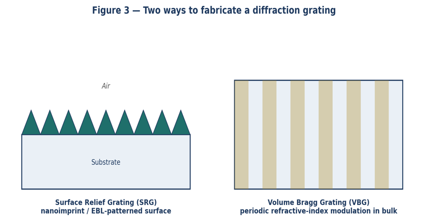
Figure 3. Surface relief gratings pattern the physical topology of the substrate; volume Bragg gratings modulate refractive index within the bulk material — different fabrication routes to the same diffractive function.
This is not a decision that can be made purely from an optical-performance spreadsheet. SRGs are compatible with high-volume, semiconductor-adjacent manufacturing techniques and tend to win on scalability; VBGs typically require holographic recording processes that are harder to parallelize at wafer scale but can deliver very high, spectrally clean efficiency where the application allows a narrower operating window. Every waveguide combiner program I’ve been close to eventually has this conversation, and it’s rarely resolved by simulation alone — it’s resolved by which fabrication route the team can actually get to yield.
10. Building a surface relief grating: from EBL master to volume replication
Because SRGs are the more common production route today, it’s worth walking through how one actually gets built. The process almost always starts with electron-beam lithography (EBL): a focused beam of electrons scans across a resist-coated substrate, exposing the pattern one nanoscale pixel at a time based on a digital design file. EBL is exceptionally precise — capable of feature sizes and placement accuracy well below what’s achievable with visible-light photolithography — but it is also serial and slow, tracing out a pattern point by point rather than exposing an entire area at once through a mask. That combination of precision and slowness makes EBL a poor fit for direct production but an excellent fit for writing a master — a single, highly accurate reference copy of the grating pattern.
Once the resist is exposed and developed, the pattern is transferred into the underlying material — commonly through reactive-ion or deep reactive-ion etching (RIE/DRIE), which uses a chemically reactive plasma to remove material selectively where the resist has been cleared, translating the two-dimensional exposed pattern into a three-dimensional physical relief. That etched master then becomes the tooling for nanoimprint lithography (NIL): a stamp — effectively a nanoscale rubber stamp — is pressed into a soft, typically UV- or thermally curable resin coated on each production substrate, physically transferring the master’s relief pattern by mechanical contact rather than by light or electrons at all. NIL is dramatically faster and cheaper per part than EBL, which is precisely the point: one slow, expensive master enables thousands of fast, low-cost replicas, similar in spirit to how a single injection-mold tool stamps out large volumes of plastic parts.
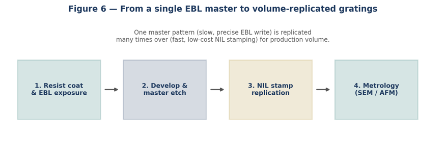
Figure 6. A slow, high-precision EBL master pattern is replicated at volume through fast, low-cost nanoimprint lithography.
Every step in this chain introduces its own tolerance budget, and those tolerances compound. EBL beam placement error, resist sensitivity variation, etch anisotropy and selectivity, NIL stamp wear and resin shrinkage on cure — each contributes some deviation from the ideal grating geometry, and diffraction efficiency is often disproportionately sensitive to exactly the parameters most prone to drift: sidewall angle, duty cycle (the ratio of ridge width to period), and grating depth. A grating design that looks flawless in an electromagnetic simulation can perform noticeably differently once real process variation is layered on top — which is why process development, not just optical design, ends up determining what’s actually achievable in a shipping product.
11. When it goes wrong: a root-cause story
I want to make the tolerance-sensitivity point concrete with an example close to my own work, because it’s easy to state abstractly and much more informative to see it play out. On one nanofabrication program I led, we started seeing a recurring, spatially periodic patterning defect across EBL-written fields — visually, something like a faint checkerboard pattern superimposed on what should have been a uniform grating array. It was subtle enough to survive an initial visual inspection but showed up clearly in diffraction efficiency measurements as unwanted energy scattered into orders it shouldn’t have populated, and it was costing real yield.
Tracking it down meant treating it as a proper design-of-experiments (DOE) problem rather than guessing. We systematically varied exposure dose, beam step size, and field-stitching parameters — the settings that control how the EBL system breaks a large pattern into smaller sub-fields and stitches them back together during the write — while holding everything else constant, then correlated the resulting defect signature against each variable individually. The root cause turned out to be a subtle field-stitching error: at the boundaries between adjacent exposure fields, small, systematic beam-placement discrepancies were accumulating into a periodic dose variation, which the resist development process then amplified into a visible, periodic linewidth variation — the checkerboard. Once isolated, the fix was a combination of a revised stitching calibration routine and a tightened field-overlap tolerance in the write job — not a change to the optical grating design at all, which had been correct from the start.
I raise this not because the specific mechanism generalizes to every process — it won’t, every tool and process stack has its own failure modes — but because the shape of the investigation does generalize, and it’s the part of this work that rarely makes it into an optics-focused explanation of AR displays. The grating equation and the étendue conservation law are both exact; the physical device that has to embody them is not, and getting from one to the other reliably, at yield, is where a meaningful fraction of an AR optics program’s engineering effort actually goes.
12. Metrology: verifying what you actually built
None of the process control described above is possible without measuring the result, and grating dimensions are small enough that this is its own nontrivial discipline. Scanning electron microscopy (SEM) is the workhorse for direct dimensional inspection — imaging cross-sections or top-down views to measure critical dimensions, sidewall angle, and line-edge roughness at nanometer resolution, though cross-sectional SEM is inherently destructive, since it typically requires cleaving or milling through the sample. Atomic force microscopy (AFM) offers a non-destructive alternative, physically tracing a sharp probe tip across the surface to reconstruct a three-dimensional topography map, useful for grating depth and duty-cycle measurement without sacrificing the part, though slower and less suited to high-throughput inline monitoring than optical scatterometry-based techniques, which infer grating geometry indirectly from how a part diffracts a calibration beam and can run fast enough for production-line sampling.
In practice, a mature grating process leans on all three: scatterometry for fast, high-volume inline monitoring; periodic SEM cross-sections to calibrate and validate what the scatterometry model is inferring; and AFM when a specific anomaly needs a genuinely three-dimensional, non-destructive look. None of these measurements are optional extras bolted onto the optical design — they’re the feedback loop that makes it possible to hold a process at the tolerances the diffraction physics actually demands.
Bringing it together
None of the fabrication reality described in Part Two changes the physics an optical architect reasons about — étendue is still conserved exactly, TIR still governs how light moves through the waveguide, and the grating equation still sets the diffraction angles regardless of whether the grating exists as a surface relief pattern or a volume index modulation. But the fabrication route chosen to realize any given grating design feeds back into what’s actually achievable: process tolerances set real, physical limits on how aggressive a diffraction efficiency or color-uniformity target can be, and yield economics frequently decide which architecture reaches a product roadmap at all, independent of which one performs best in an idealized simulation.
The optics tells you what’s physically possible. The fabrication process tells you what’s actually buildable, at a price and yield a product can survive on. Getting from a working prototype to a shippable device means holding both of those constraints in your head at the same time — and in my experience, it’s very often the second one, not the first, that ends up on the critical path. That’s the corner of photonics I find most interesting the deeper I go into it, and it’s the thread I plan to keep pulling on in future posts.
Further reading
Kress, B. C. Optical Architectures for Augmented- and Virtual-Reality Headsets. SPIE Press, 2020.
Kress, B. C., and Chatterjee, I. “Waveguide combiners for mixed reality headsets.” Nanophotonics 10, no. 1 (2021): 41–74.
Hecht, E. Optics, 5th ed. Pearson, 2016. (Foundational treatment of diffraction, interference, and total internal reflection.)
Maimone, A., and Wang, J. “Holographic optics for thin and lightweight virtual reality.” ACM Transactions on Graphics 39, no. 4 (2020).
Levinson, H. J. Principles of Lithography, 4th ed. SPIE Press, 2019. (EBL, photolithography, and process-tolerance fundamentals.)
Chou, S. Y., Krauss, P. R., and Renstrom, P. J. “Imprint lithography with 25-nanometer resolution.” Science 272, no. 5258 (1996): 85–87. (Foundational nanoimprint lithography reference.)
Schubert, E. F. Light-Emitting Diodes, 2nd ed. Cambridge University Press, 2006. (LED device physics, IQE/EQE, and efficiency droop mechanisms.)